Recently I’ve been experimenting with Attiny microcontrollers for a project that might get its own post at some point. For that project it’d probably be easiest to have a pcb to hold all components in place. A bit of googling lead me to KiCad.
KiCad is “A Cross Platform and Open Source Electronics Design Automation Suite” and seems to be a popular PCB design tool, and is seen as very powerful. So I invested some time into learning the basics, and managed to get a pcb design done. This post is meant to describe the basic workflow. Keep in mind that I’m neither and electrical engineer, nor a KiCad expert, so this just describes what worked for me, and probably won’t match best practices.
General Workflow
KiCad has a workflow that seem complicated at first, but makes sense once you wrap your head around it. Designing a PCB requires you to have a schematic of the ciruit first, for this you’ll use Eeschema.
Once you’ve designed your shematic, you assign specific components to each symbol (For example 0805 SMD for a resistor). With components assigned, you can generate what’s called a “netlist”, which is essentially the component list for the PCB. This list can then be imported into PCBNew (the PCB designer), and then you layout, connect your traces, etc.
The main window
Once you’ve started KiCad and created a new project, you should see something similar to the following:
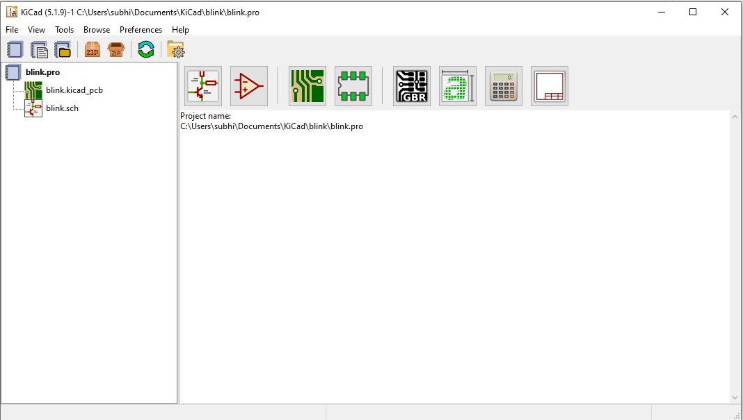
On the left side, there’s a list of all files that belong to your project. You can double-click these to open them in their related tool (Eeschema or PCBNew for example). The buttons above the white block in the middle give you access to Eeschema and Pcbnew, but also footprint and symbol editors and some other utilities.
Designing the schematic
The first step of the process is designing the schematic, this will happen in Eeschema. To launch it, either double-click on the .sch file or on the leftmost button above the blank space.
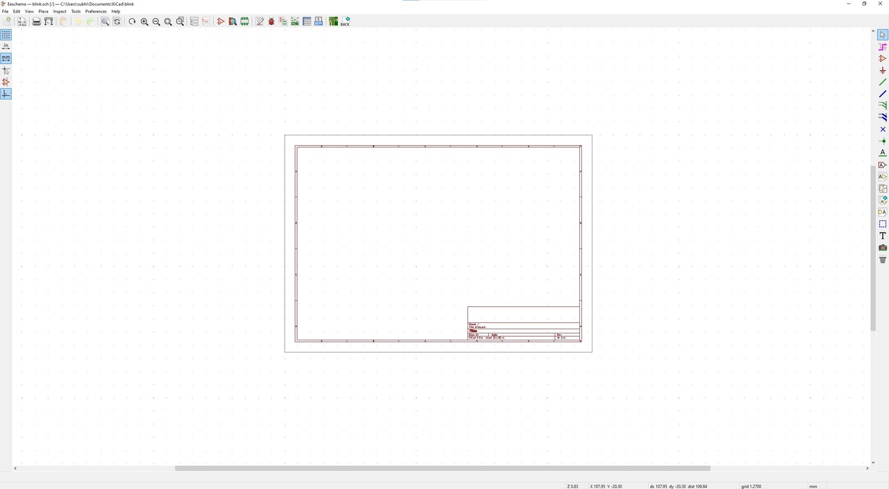
First, place your symbols (components) using the Place Symbol tool in the right menubar
 . Connect these using the wire tool
 .
.
You’ll also need to add your ground and vcc sources with the power tool
 .
.
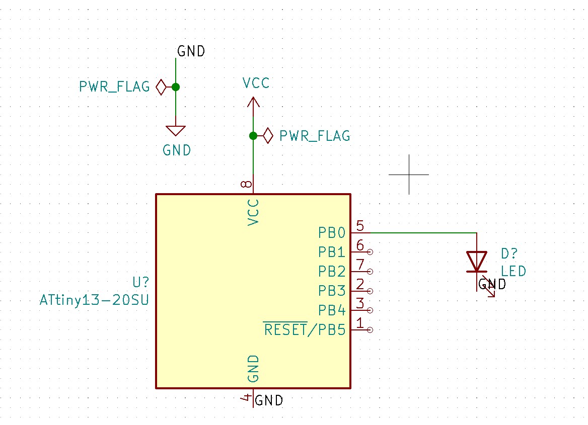
Once you’ve placed your symbols and power sources, you could end up with something like this:
 .
.
Note the “PWR_FLAG” components, this tells the KiCad electrical error checking tool where our power comes from, this is a psuedo-element just to make sure KiCad can understand your diagram better.
Another interesting feature is that nothing is connected to ground, instead, items that should lead to ground have the “GND” label. Everything with the same label is seen as connected to each other, this saves you from drawing lines to for example ground everywhere. Labels can be applied using the “Place net label” tool
 .
.
With all of this done, the next step is to annotate the components, the question marks after “D?” and “U?” denote that these symbols still need to be annotated, which is essentially just naming them for the pcb silkscreen. You can have this done automatically with the “Annotate symbols” tool in the top menubar
 . This will open a window, if you click “Annotate” your symbols should now be numbered.
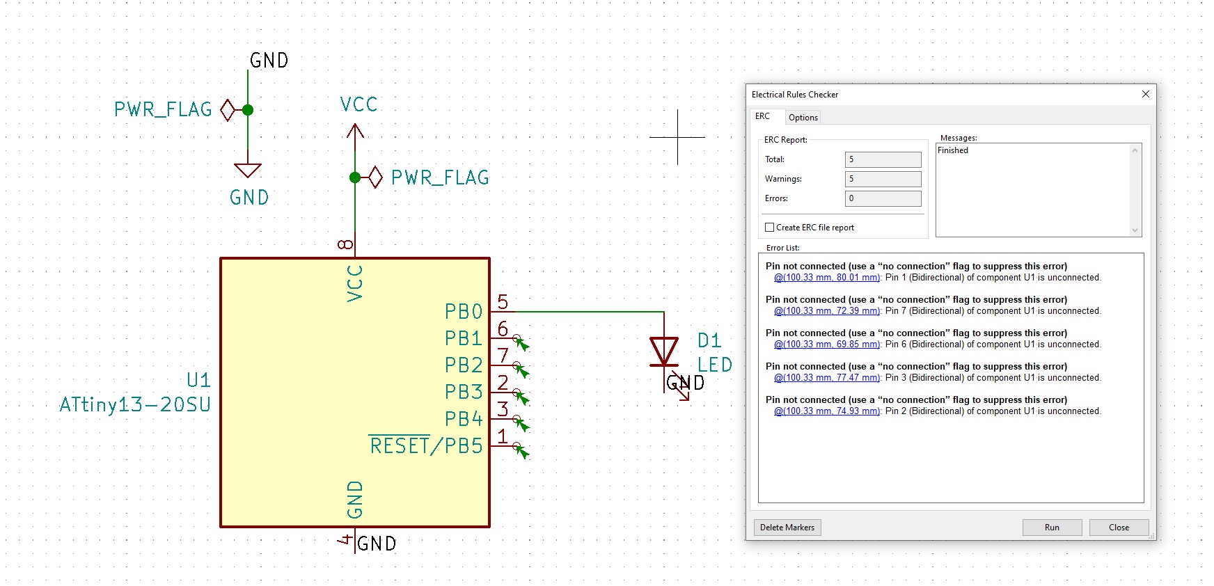
The next step is to perform the electrical rules check
 .
, this will check if everything is wired up, and if there are any other errors.
 .
.
In the window above, we can see we have warnings for unconnected pins, to fix this, we can add the “No connection”
 .
flag as suggested by KiCad, informing it that these pins are meant to be unconnected.
At this point, running the ERC again should result in 0 warnings.
Assign PCB footprints
Now that we have a complete schematic, we need to assign footprints
 to our symbols, these are the components that will actually be on the pcb, and are used to determine where the solderpads go.
Clicking this will spawn a new window that might take a while to populate, after which you’ll see your symbols in the middle, available footprint libararies to the left, and matches within that library to the right.
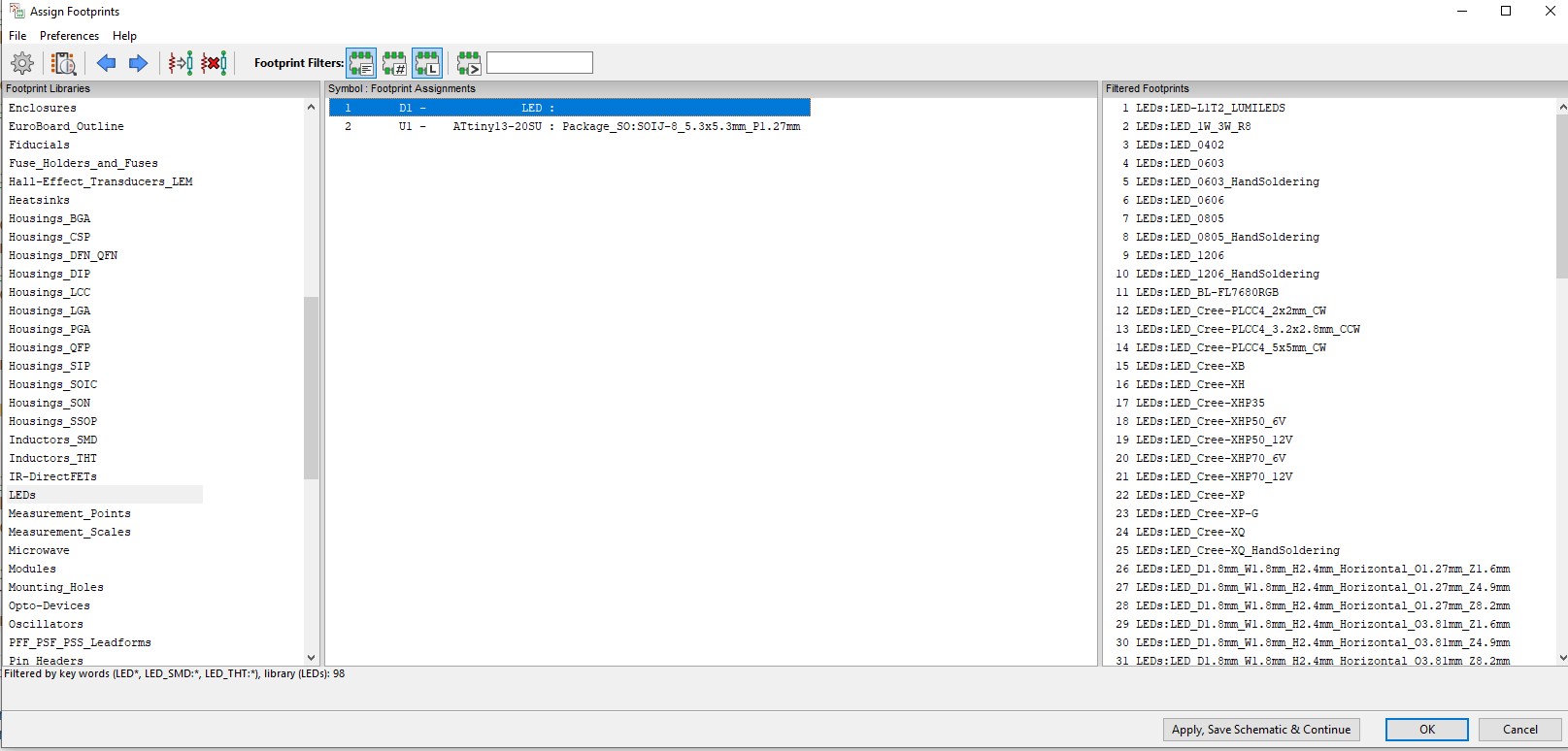
In the example above, we can doubleclick to pick the exact component for our LED, and our ATtiny already had a component assigned.
With that complete, all we need to do is generate a netlist
 ,
after which we can quit Eeschema and move on to Pcbnew.
Pcbnew
From the main Kicad window double-click your .kicad_pcb file. This should greet you with the following window:
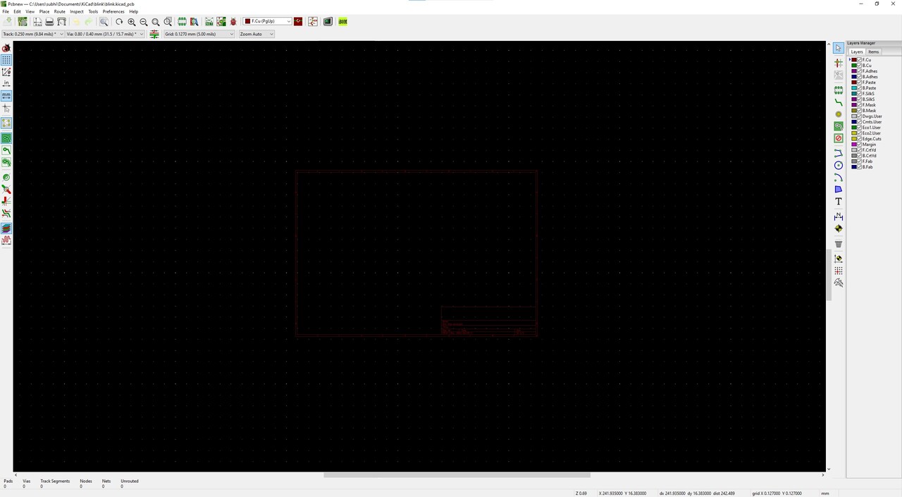
Pcbnew is the tool we use to actually create the PCB. It looks a bit empty at this stage however, so the first thing to do is to read the netlist we generated with Eeschema earlier. This can be done using “Load netlist”
 .
.
Once you’ve loaded your netlist, you should see actual footprints somewhere in your working area:
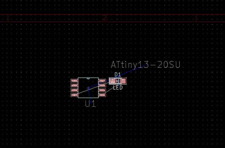 .
.
Now that you have your components on your pcb, the next step is to add tracks
 .
to actually connect them together.
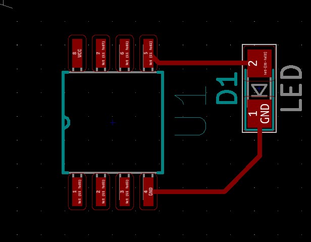 .
.
Adding edge cuts
Finally, we need to switch to the edge cuts layer to tell Pcbnew what dimensions and shape we want our pcb to have.
 .
.
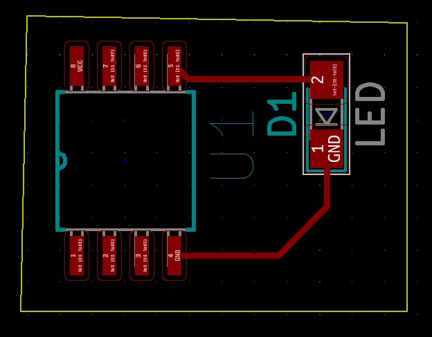
Now we need to draw where the edges will be cut using the “Add graphic lines”
 tool. Draw lines around the edges of your components, in the shape you want your pcb to be.
 .
.
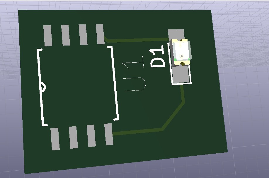
Pcbnew also comes with a 3d viewer under “View -> 3D Viewer”. This will open a new window with a preview of your pcb.
 .
.
Gerber export
If you’re happy with your PCB, you’ll need to export it. A fairly common format for PCB fab houses is the gerber format, KiCad can generate gerber files using the Plot
 tool. Clicking the plot tool will open a new window.
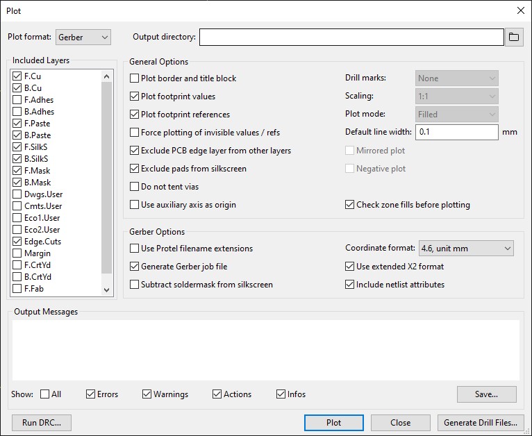
The PCB fab house you’re using should have specifications and maybe KiCad specific config for the gerber output. Set the config in this window to match those instructions. Once you’re happy, fill in the output directory (if you just type a name, it will create that directory relative to the current project), and click Plot.
Once that’s done, in your main KiCad window, you should have the gerber files visible:
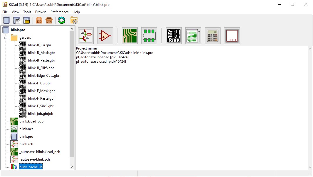
That’s the basic process for designing a PCB in KiCad, which you can then have produced by a PCB fab house.